Sputtering Targets List
Sputtering is one of the main techniques for preparing thin film materials. First, ions are generated by ion source. Then, they are accelerated in vacuum and a high velocity energy ion beam is formed, which will bombard the solid surfaces. Finally, kinetic energy exchange occurs between atoms of the solid surface and ions, so that the atoms on the solid surface leave the solid and deposit on the basement surface. The solid being bombarded is the raw material of the film deposition by sputtering technique, which is called sputtering targets. Various types of sputtering film materials have been widely used in many fields. Therefore, the demands for sputtering targets is increasing year by year.
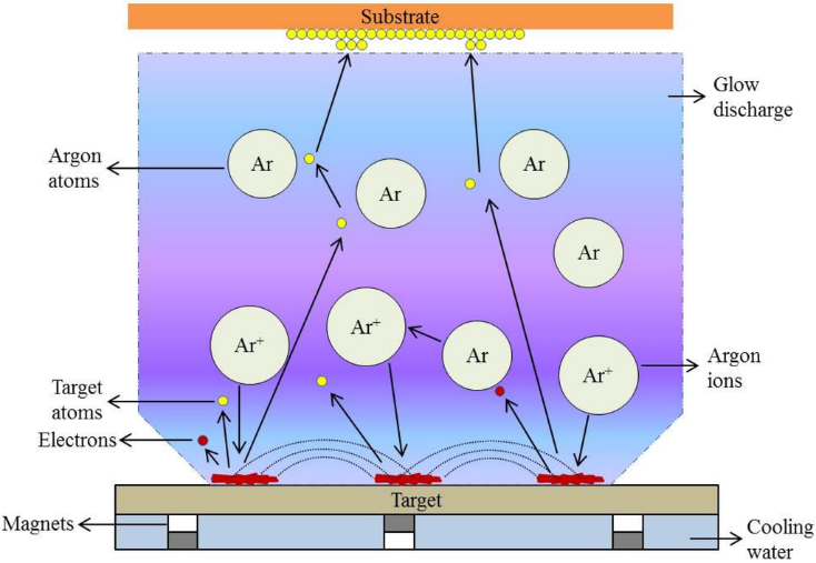 Figure 1. Illustration of sputtering technique process.
Applications:
Sputtering targets are widely applied in many filed, including electronic and information field, glass coating field, high-grade decorative products filed and the others.
- Information storage field: With the continuous development of IT industry, the demand for recording media is increasing, and the research and production of target materials for recording media has become a hot spot. In the information storage field, thin film products made from sputtering targets include hard disk, magnetic head, optical disk and the others. Sputtering targets with high quality, special crystallinity and special composition are needed for manufacturing of these data storage products. The commonly used sputtering targets include cobalt, chromium, carbon, nickel, iron, precious metal, rare metal, medium materials, and the others.
- Integrated circuit field: Sputtering targets are important for integrated circuits, and the sputtering products mainly include electrode interconnect film, barrier film, contact film, optical disc mask, capacitor electrode film, resistance film, and the others. Among them, resistance film is the most used element in the film mixed integrated circuit.
- Flat panel display field: Flat display mainly includes liquid crystal display (LCD), plasma display (PDP), field luminescence display and field launch display (FED), which can be widely used in laptop computer monitors, desktop computer monitors and high-definition television. The thin films of planar displays are mostly shaped by sputtering technique. and the sputtering targets generally include In2O3, SnO2, MgO, W, Mo, Ni, Cu, Cr, and the others.
- The others: Sputtering targets are also can be applied in other fields, such as glass curtain wall and car rearview mirror coating. For example, a special film system used in car rearview mirror coating is plated by magnetron sputtering and the reflected light is very soft and clear.
Classification:
There are many kinds of sputtering targets and classification methods are varying. According to the application field, sputtering targets can be divided into microelectronic target, magnetic recording target, optical disk target, precious metal target, thin film resistance target, conductive film target, surface modified target, light cover layer target, decorative layer target, electrode target and the others.
Reference
- Maurya, D.K.; Sardarinejad, A.; Alameh, K. Recent Developments in R.F. Magnetron Sputtered Thin Films for pH Sensing Applications—An Overview. [J] Coatings. 2014, 4, 756-771.
